
Within the context of today’s rapidly changing technology, the issues of power integrity and signal integrity have become fundamental to system-level design and implementation. This is useful to engineers or designers who consider making durable and effective devices. This blog covers the relevance of power and signal integrity, their impacts, and how to achieve them and other nonstandard performance in modern electronics.
Defining Power and Signal Integrity
According to the power supply integrity definition, it implies that all intended devices in the electronic system work under a fixed, grounded, and noiseless voltage level. This includes properly controlling the voltage, not allowing noise, and making sure power distribution networks (PDN) can support the power level without sagging this level. Power integrity is important because any fluctuation of power supply can cause system critical component failure, loss of precious data or worse system failure.
The Definition of Power Distribution Networks/Power Distribution Network (PDN)
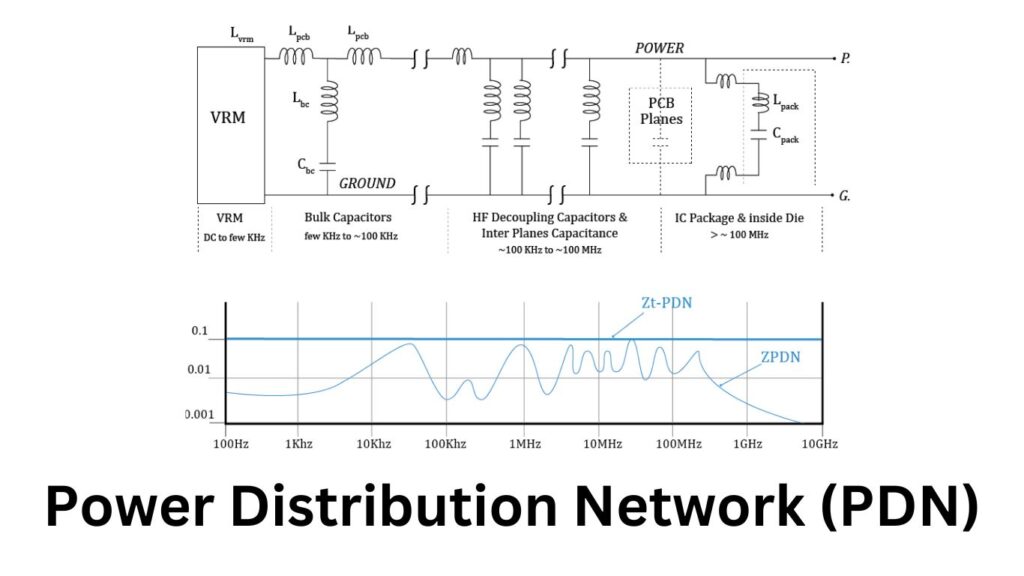
Power distribution networks (or PDNs) are quite significant in controlling power integrity. Such networks usually comprise capacitors and inductors among other elements to enable the distribution of power efficiently through a circuit. With respect to this, designed PDNs always reduce the drops or deflections in the voltage and, hence, allow all the parts of a circuit to get enough power for correct operations. The design of PDNs requires studying parameters such as impedance, capacitance, and module disposition to avoid compromises with efficiency.
The Concept of Maintain Quality of Circuits
Signal integrity relates to the likelihood of a usable electrical signal at the output nodes of the circuit. It concerns with what is known as controlling the signal to the level that it is sent or the point to which it is conveyed. High degrees of signal integrity help to certify the validity of the data passed to the user or from the user, which is very important in high-speed digital systems.
Factors Affecting Power and Signal Integrity.
There are a number of such factors that can affect signal integrity: transmission line effects, crosstalk, electromagnetic interference (EMI), and reflections. These elements can add some or the other noise creating data errors. For example, there are resistances and capacitances, which cause a degradation to the user when a signal runs over a long trace. Thereafter, it’s relevant to consider these factors during the design stage in order to avoid sooner or later arising problems.
The Relationship Between Power and Signal Integrity
Power integrity and signal integrity are closely related, as problems of one type will invariably have implications for the other. Thus, power supply instability results in signal distortion on mosfets via voltage spikes within nets carrying logic signals. However, a low quality signal integrity could interfere with the power up the output and into the components. Such relations make it impossible to ignore the design of the whole system.
Best Practices for Ensuring Power and Signal Integrity
There are some best practices that can be followed by the engineers in order to maintain proper power and signal integrity.
- Use Decoupling Capacitors: These capacitors are effective at eliminating high frequency decoupling noise and controlling power distribution to the power pins of complexes.
- Optimize PCB Layout: A properly designed printed circuit board (PC) layout not only shortens the trace length but also employs ground planes to cut down the level of electromagnetic interference.
- Put into practice Controlled Impedance: It mitigates the reflections of the traces to maintain the integrity of the signal as well as the consistency of the propagating signal with the help of controlled impedance designs on traces.
- Minimize Crosstalk: There CCAs in the engineering domain state that placing distance between the signal traces provides signal integrity not only between the signal traces making it into I/O planes even when they are within one substrate and especially with regard to differential planes.
- Perform Simulation and Analysis: When there is virtually no power and signal integrated circuitry, CAE tools can optimally execute design tasks, making circuit board designs without having physically fabricated the prototypes.
The Importance of Simulation Tools in Power and Signal Integrity
Power and signal integrity have changed for the better with the help of simulation tools among engineers. The tools make it possible to go to the extent of analyzing the behavior of the circuit under all possible factors which in turn would help avoid the problems. Engineers are able to apply backend solutions, optimization and other related strategies to enhance the electrical power as well as the signal integrity of the systems. These are achievable through the simulation of the systems even before they are put into practice.
The Future of Power and Signal Integrity
The advances in technology keep burning the need for electronic products that are not only high speed but also high performance. This trend therefore amplifies why read deeper into power and signal integrity. But developments in relation to indicate that other phenomena are likely to develop high demand than ever power and signal integrity in relation to 5G, IOT, AI et al.
The 4 Types of Power and Signal Integrity Problems
1. Electromagnetic interference (EMI)/electromagnetic compatibility (EMC)
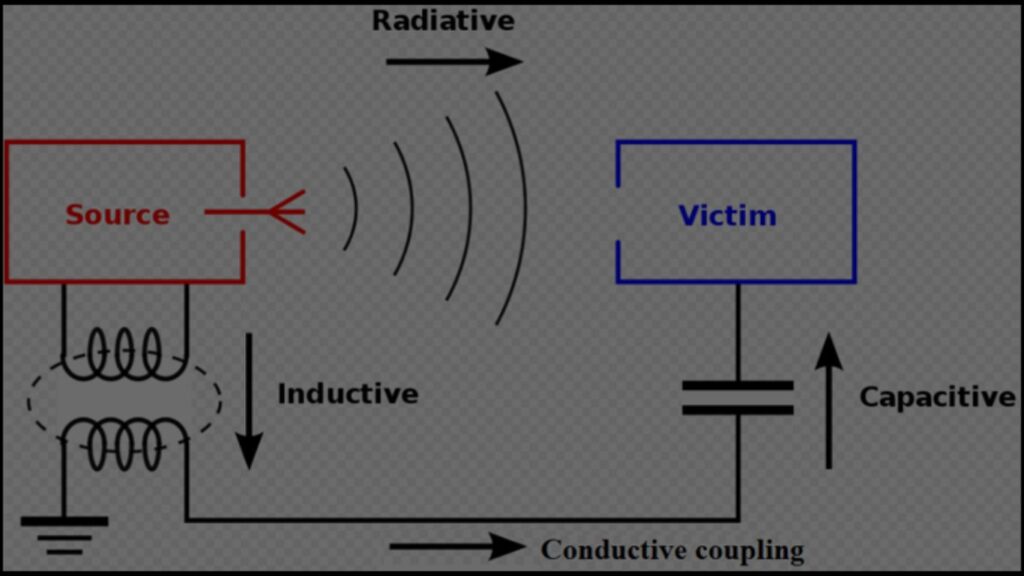
Interference Electromagnetic (EMI) pertains to the performance of electronics equipment being disrupted due to unwanted signals from electromagnetic sources around it. These can stem from Mother Nature lightning for example or from one or several of a man-made mischievous sources, such as motors, radios, and power lines states that according to the international quality standards EMI may affect sensitive devices resulting in reduced performance or even worse its failure.
Compatibility Electromagnetic A electromagnetic signature of a specific piece of equipment is the equivalent of a human footprint in the sand the width length and depth are all unique. When multiple devices and systems are placed in close proximity to one another and turned on there is the potential for distortion and interference. Distortion and interference can result in malfunctions, degradation to performance, or destruction or damage to a piece of equipment or interface ICS states that EMC means that a design or devise has been tested and confirmed to work correctly along other devices in an electromagnetic environment.
Key Points About EMI
Conducted EMI: Interference transmitted through cables or conductive paths.
Radiated EMI: Interference emitted as electromagnetic waves through the air.
Common Sources of EMI:
Electric motors, transformers, and power lines.
Wireless devices like radios, mobile phones, and Wi-Fi routers.
Industrial equipment and switching power supplies.
Have A Broader Understanding About EMC
Emissions is the degree of noise that a device allows its processor and environment to consume states that noise includes electromagnetic interference.
The ability of a device to block out interference external sources refers to shielding.
Empirical shielding cables when around circuits to suppress radiated emissions interference states filtering power supplies reduces or alleviates conducted interference.
The importance of PCB design layout, component placement and grounding.
Application
Automotive: Focusing on sensors and infotainment, ensuring their mutual disturbance is sufficiently low.
Medical Devices: Providing protection for life critical devices such as a pacemaker.
Aerospace: Preventing the occurrence of EMI in navigation and communication systems.
Consumer Electronics: Desired EMC is achieved for FCC and CE compliance.
All in all, relevant design characteristics and proper EMI/EMC management is required for appropriate functioning of next generation electronics systems.
2. Crosstalk
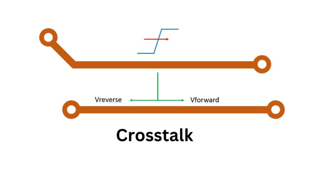
In telecommunications, electronics, and data transmission networks, crosstalk can negatively affect the performance of various devices. It has been established as an unwanted signal that is caused by inter-window or intra window disturbances or sometime even by the cross-talking of channels induced by a voltage or current over cross talking circuits over numerous lines.
Types of Crosstalk
Near-End Crosstalk (NEXT):
Apart from their respective distance from the crossover, Now Maintaining definition, Near-Eden crosstalk arises when interference is induced at the transmitting end of the line. Crossover circuits in telecommunication systems that are closely packed cables are common cases of these near – end crosstalk interference.
Far-End Crosstalk (FEXT):
For signal stability, electromagnetic interference is a crucial design concern in high speed data networks. This occurs at the receiving quarter of the link line.
Effects of Far- End Gain
This F- gain which occurs at the far end of a solenoid winding or at the far end terminal on the transmission link accentuates the feelings received at the global receiving terminal.
Reasons of Crosstalk
Electromagnetic Coupling: Proximity of conductors or circuits results in wires or circuits influencing others behind their desks.
Impedance Mismatch: Multitude of signal interfering evaluated with poorly designed or poorly terminated connections.
Poor Shielding: Cables with weak shielding are more likely to experience interference that bypasses magnetically that other coaxial cables with strong shielding around them.
Consequences of Crosstalk
Signal Integrity: Deteriorates the level of quality and accuracy of the data sent or received.
Increased Errors: Reduction of performance tries to mitigate the loss of packets, delays in communication and pushes for re-transmissions in the data networks.
Performance Issues: Greatly affects the accuracy of the system in delicate instruments especially audio devices and a range of medical devices.
How to Mitigate Crosstalk
Cable Design: The use of twisted pair cables to cancel out electromagnetic interference.
Shielding: The use of shielded cables or enclosures to avoid coupling.
Physical Separation: To increase space between the signal lines.
Proper Termination: To use proper impedance matching to reduce the reflection and interference.
Signal Filtering: Use filters to block all signals except for the desired and filter out the noise.
Industries Who Are Prone To Crosstalk
Telecommunications: Clarity of the signal while handling telephones and internet system.
High Speed Data Networks: Perform reliably in Ethernet and fiber optics.
Audio Systems: Forbid sound from one channel from leaking other channel.
PCB Design: Keeping all the components of the circuits in a dense circuit layout but with reduced interference.
Crosstalk management is vital as far as the integrity of the signals is concerned as well as the reliability of the system in modern technology.
3. Simultaneous switching noise (SSN)-caused ground bounce
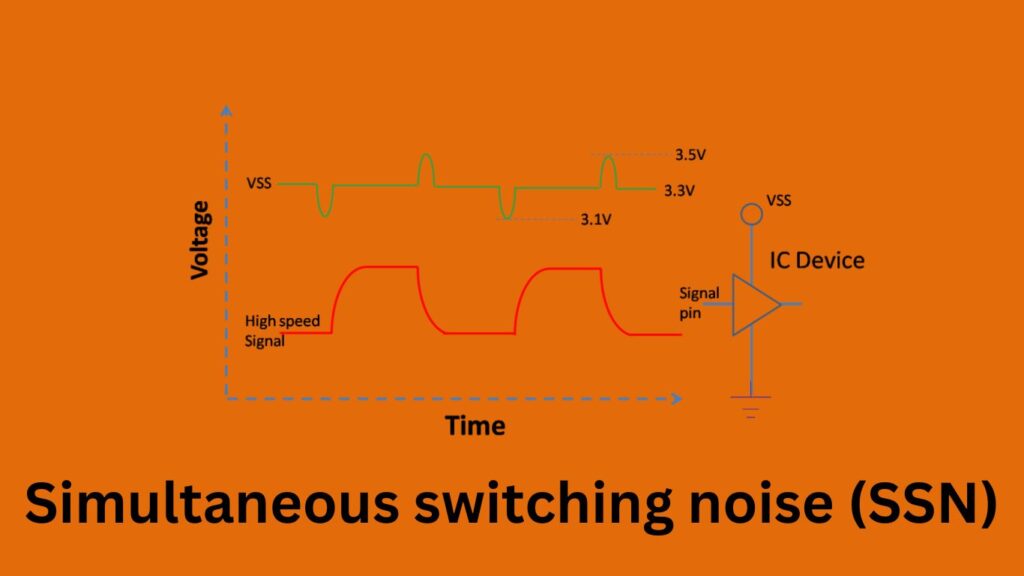
Simultaneous Switching Noise (SSN), which is sometimes referred to as “ground bounce”, affects digital circuits and systems whenever there is quick switching of output drivers from low to high (or high to low) mostly in circuits with multiple output drivers. The switch of states is rapid, hence, it influences the performance of any circuit, and with time, may cause unreliability of the circuit by introducing transient noise to the power and the ground planes.
Mechanism of Ground Bounce
1.Simultaneous Switching: A surge is created by electrically connected transistors or drivers that can transfer large electrical currents but all together at a given period
Inductive Reactance: When a circuit trace or package’s lead inductance virtually changes because of the sharp current change, a voltage drop occurs which is:
Voltage Fluctuations: Voltage Fluctuations: shunting or inductance shifts negative voltages from the power earth plane, causing reference shift in the middle of the circuit and subsequently developing noise during application of electric signals.
Effects of SSN and Ground Bounce
Interference in the ground between other active traces creates high frequency noise, resulting to ground bounce voltage.
Logic Errors are prevalent when SSN occurs as it induces glitches or false triggers within the circuitry.
In data error ensuing disintegrate the timing margin is a decrease in the signal quality due to SSN.
Crosstalk otherwise promotes the alteration in the coupling noise of interspersed channels/ traces.
Over the period of time, components are bound to develop reliability issues due to repeated stress on these components.
Mitigation Techniques
Decoupling Capacitors: Surround the power pins with capacitors that supply power locally when the device is about to flip.
Power/Ground Plane Design: Low-inductance planes with a certain thickness and a specific order of layers should be applied.
There is a need to control and restrict the speed of switching on and off to sufficient levels to lower
Staggered Switching: Rather than having all outputs switch at once, they will instead overlap multiple clock cycles.
Use of Ground Pins: Provide additional ground pins within package of ICs to provide less inductance to be shared.
PCB Layout Optimization: Short, wide traces for ground and power connections. Confirm to make sure loop areas are kept to a minimum.
4. Impedance Mismatch
An impedance mismatch is described as a source, transmission line or a load having different impedance, a fraction of the transmitted signal is bounced back to the source. This physical phenomenon is largely found in electrical and electronics circuitry systems, in particular, when high frequency signals need to be transmitted such as in RF systems, during the transmission through communication lines and also in high speed PCBs.
Key Causes of Impedance Mismatch
Different Impedances: The connected devices and wires has varying impedances.
Termination Problems: Termination resistors are absent or incorrectly connected at the end of a line.
Length and Type of Cable: The used transmission lines or the cables have different lengths.
Design of Connectors: Connectors has different impedance for transitions.
Layout of PCB: Traces or via are located in a way that they produce impedance discontinuities in the board.
Effects of Impedance Mismatch
Signal Reflection: Part of the signal energy is reflected, thus making it to travel back into its source which leads to interference.
Signal Loss: Effect of the reflections is that a part of the signal energy cannot be utilized leading to lower efficiency.
Impulses: The signal waves are subject to setbacks and they cause standing waves which extend the duration of the signal sprays.
Poor signal quality: Meaning enough timing errors dedicated target time, jitter and ripple effects on the signal’s high speed or RF elements.
Reduced Data Transfer Quality: High error rates of communication systems
Mitigation Techniques
Impedance Matching: Employ circuits to correct the misalignment between source, line and load impedance.
Proper Termination: Use proper resistive termination that reduces reflections
Transmission Line Construction: Achieve a metric length of the line in terms of the impedance
Controlled Board Layout: Correct values for trace width, spacing and routing with parameters of such circuits
Use of Baluns: Allow to pass from unbalanced to balanced systems and vice versa
Applications Where Impedance Matching is Critical
Telecommunications: Ensures minimal signal loss and reflection in coaxial cables or fiber optic’s
RF Circuits: Maintains efficiency in antennas, amplifiers, and transmission line’s
High-Speed Digital Systems: Ensures proper data transfer in DDR memory and PCIe interface’s
Audio Systems: Prevents signal loss or distortion in microphone and speaker setups.
Conclusion
To sum up clearly, power and signal integrity are as essential as bread and butter in terms of interfacing systems. Understanding these principles and implementing these issues can help engineers work more smartly to develop utilizations of such engineers’ solutions more effectively and intelligent systems in power and signal integrity for the future. In this fast-paced world of electronics design and development where technology keeps changing, keeping abreast of changes in power and signal integrity will be of utmost necessity in the near future. Therefore, embracing these concepts will enhance further advancements and performance in the electronics sector.
This blog post, therefore, aims at exploring the concept of power and signal integrity in the electronics field while also optimizing for search engines by using structured formats and appropriate keywords. If there’s anything else or anything further you’d prefer me to write about, don’t hesitate to tell me!
Visit our latest Blog about (Magneto Motive Force (MMF): The Ultimate Guide to Electromagnetic Efficiency) Any question regarding to this article please contact us.
FAQs (People Also Ask About Power and Signal Integrity)
Q1.What are power and signal integrity, and why are they important in modern electronics?
While power integrity deals with the quality of the power provided to the electronic systems, signal integrity is concerned with electrical signals as propagating across the circuit. Both of them are key to ensure that a given device does not have reliability issues, efficiency issues, and start working in a suboptimal manner, especially at the case of high speed or more range complex systems.
Q2.How do power and signal integrity affect the performance of electronic devices?
Not having power integrity would cause fluctuations in voltage caused breeds instability within the system and cause noise, or even failure. Signal integrity on the other hand being a problem would lead to a miscarriage of signals yen a given device resulting in increased response time and poorer performance and even miscommunication of components. The two have an impact of the overall functioning of modern devices and the reliability.
Q3.What are common challenges engineers face when maintaining power and signal integrity?
Engineers are restrained due to factors like noise in the power supply, voltage drops and fluctuations of the current. Signal integrity issues include crosstalk, reflections and degradation of the signal due to transmission line effects or improper grounding. These problems become harder to solve as the circuits get smaller and faster.
Q4.How can poor power and signal integrity impact the reliability of an electronic system?
The damage that low-power integrity and low-signal integrity can cause includes system downUme and component throughput degradation which leads to the reduction of time to failure. Consider collaborating with the mission critical applications engineers especially in telecommunications, automotive and medical electronic devices.
Q5.What are some strategies for achieving optimal power and signal integrity in system-level design?
Optimal design practices includes power supply decoupling and providing a good reference ground while eliminating sources of noise, and using proper components and better PCB design which will limit signal attenuation and other PCB related interference requirements. Simulation and prototyping and modifying the tools are required to expose the integrity problems and possible causes at the early design stage.
Q6.How do power and signal integrity influence the durability of electronic devices?
This is how components and devices make sense. Components and devices life cycles are made optimum by power and signal integrity because issues like shock, overheating, voltage transients, and distortion are well handled. Components and devices whose signals and power supply qualities are stable suffer few failures and have long operational cycles.
Q7.What role do power and signal integrity play in high-speed digital circuits and communication systems?
In particular, high-speed circuits demand power and signal integrity because high signals have to be transmitted without distortion and interference. When signals are distorted there will be errors in all forms of communication loss of power integrity will result in the ability of high speed processors, processors memories, relevant communication links to operate accurately thus enhancing data reliability and integrity within the systems.
Q8.How do engineers ensure signal integrity in complex, high-frequency applications?
Engineers employ methods such as controlled impedance routing, differential signaling, shielding and filtering to enhance signal integrity in high frequency applications These techniques assist to minimize loss, reflectance and electromagnetic interference which tend to affect the quality of signals at high speeds.
Q9.What are the latest tools or techniques for improving power and signal integrity in advanced electronics?
With the aid of modern tools such as simulation soft wares ie HyperLynx, spice among others, numerous integrity challenges can be addressed and avoided beforehand for instance before actual hardware is fabricated. The Other applications such as on-chip voltage regulation, power-aware design, high quality digital systems construction, and advanced PCB layout techniques are used to enhance power and signal integrity.
Q10.How can power and signal integrity be affected by environmental factors like temperature or electromagnetic interference?
As the temperature rises or falls, the stability of the supply voltage and the timing of the signal can change, which can then change how the component performs. Electromagnetic interference (EMI) caused by the devices near the system can also corrupt the signals. To solve these problems, engineers provide certain measures such as shielding and grounding as well as adequate design measures.